Latest images
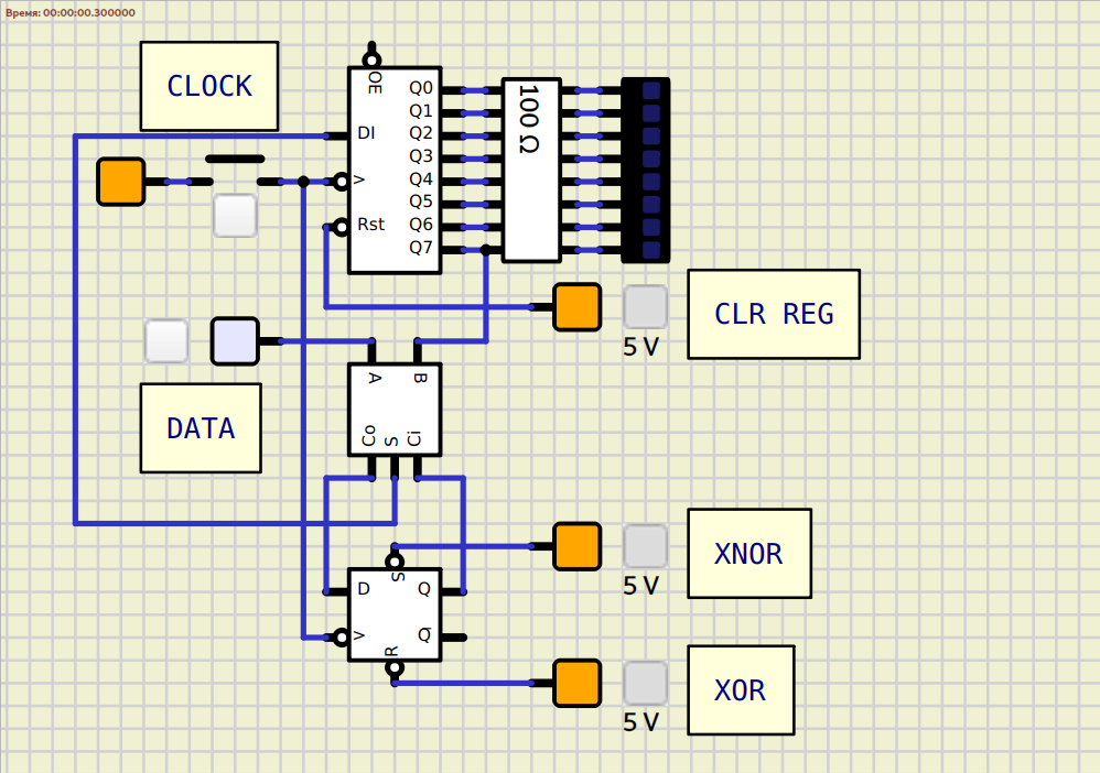
One data byte goes from the switch (LSB first), other - from the same register in which the result will be. It can add up like this: first the first number is loaded, adding up with the initial zero and gets into the register, and then the second number is added up with the first one coming from the ring. If "1" forced on the trigger, then the output will be bitwise XNOR instead of addition, forced "0" - bitwise XOR.
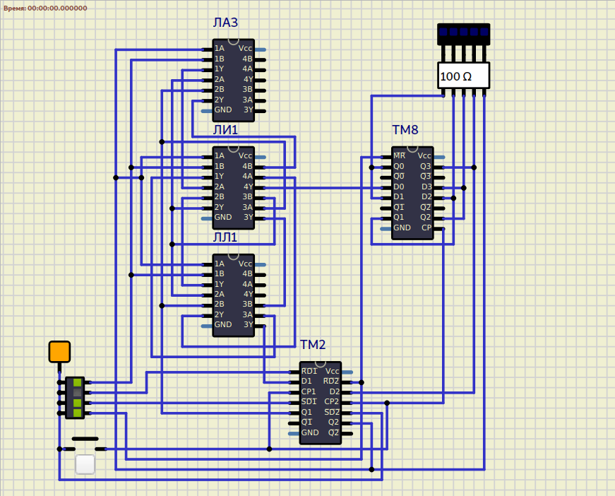
The same, but 5-bit on 74(a)ls soviet series with full adder on discrete logic:
Second half of dual D-type flip-flop is part of register.
For debounce also was made RS flip-flop on the two remaining NAND in reality.
- Attachments
 FA.zip
 - .simu files
- You don't have permission to download attachments.
- (8 Kb) Downloaded 8 times